
ON Semiconductor | AIM Photonics – TAP Facility Labs and Cleanroom
Opened in 2018, this is world’s first open-access test, assembly and packaging (TAP) facility for firms working to develop 300-mm silicon photonics wafer technology for integrated circuits.
Photonic circuits, which function using light, provide a faster alternative to electronic circuits for applications like telecommunications, computing, medicine and defense. A consortium focused on advancing U.S. photonics technology, AIM Photonics (the American Institute for Manufacturing Integrated Photonics) located their TAP facility in Rochester given the area’s expertise in optics, photonics and imaging.
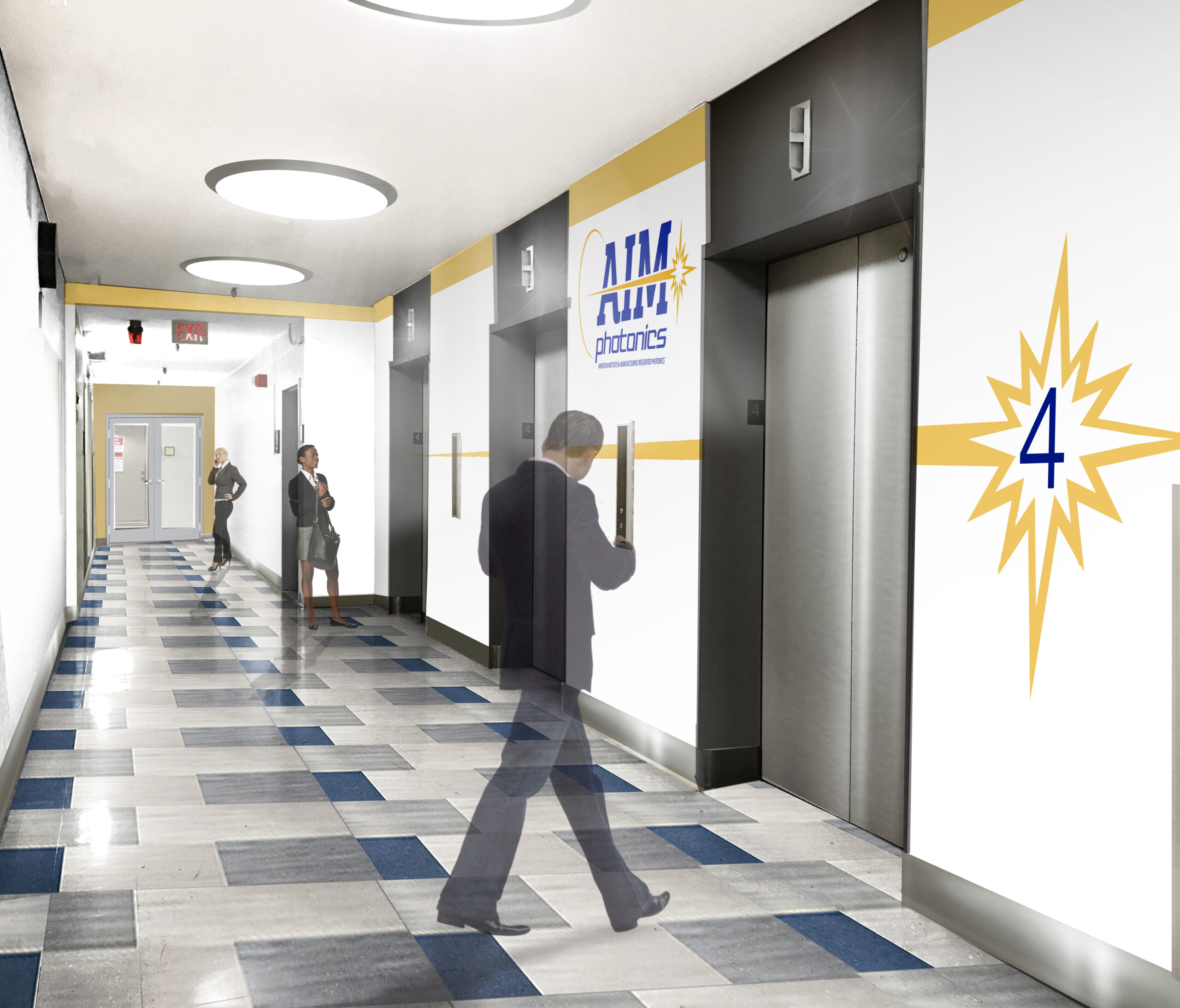
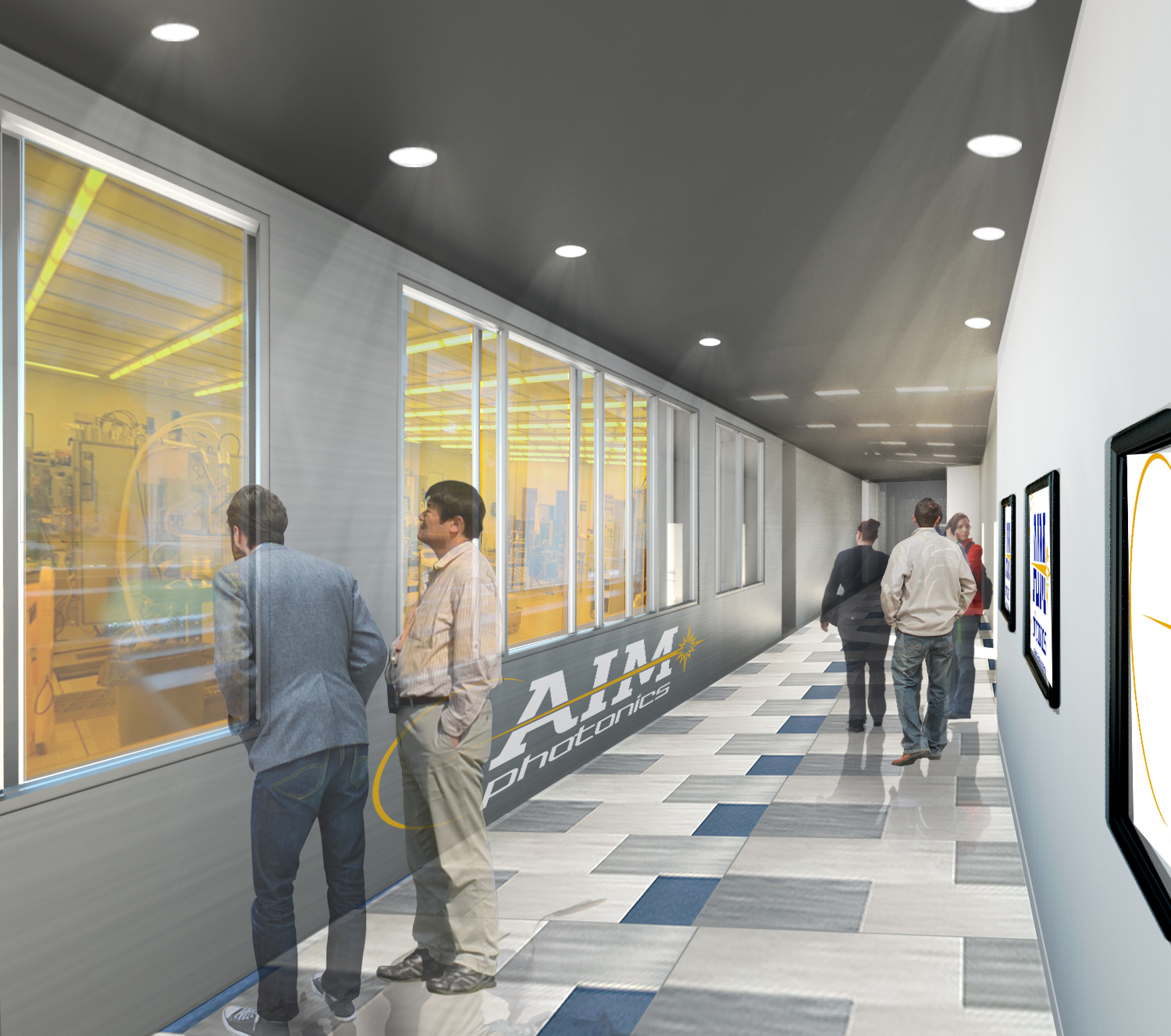
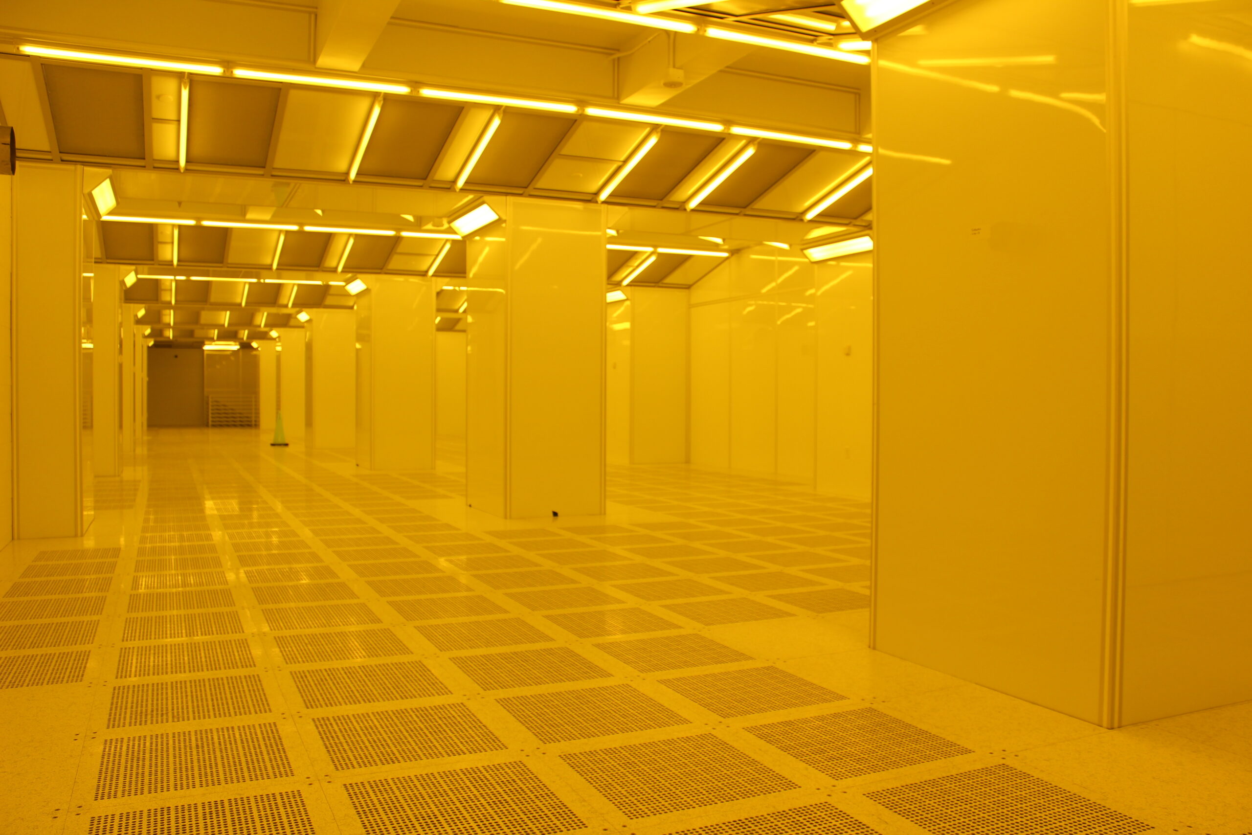
LeChase worked to completely gut, abate and rebuild the 4th and 5th floors of ON Semiconductor’s Lake Avenue building to create new offices, lab space and class 1000 cleanrooms for the TAP facility. Teams also installed new HVAC, exhaust and chilled water systems as well as process utilities to provide specialized power, nitrogen, compressed air and ultra-pure water.


")